Shielding measurement of electrically large enclosures with contents
Funder: Huawei Technologies
Date: November 2014 - September 2016
Web pages: York Research Database
My roles: Co-investigator, researcher
This collaborative project between Huawei Technologies and the AEG developed and implemented prototype production enclosure shielding effectiveness qualification methodologies for certification of information and communication technology (ICT) enclosures at frequencies from 1 to 26 GHz.
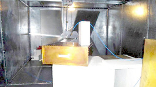
View inside the AEG’s small reverberation chamber used for characterising PCBs.
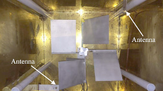
An enclosure shielding measurement setup in the AEG’s large RC.
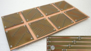
A PCB surrogate designed to match the effect of real PCBs.
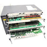
Current enclosure shielding effectiveness measurement standards, such as IEEE 299.1 assume that the equipment enclosure is empty during the assessment. Modern ICT equipment enclosures are densely packed with printed circuit boards (PCBs), power supplies, fans and other components. The internal electromagnetic field distribution in a populated enclosure is dramatically different from that in the same enclosure when it is empty due to the more complex topology and absorption of electromagnetic energy in the internal components. Since both the reliability of the equipment in the presence of external electromagnetic interference and the electromagnetic emissions of the equipment itself are dependent on the internal loading of the enclosure it is therefore necessary to develop a qualification methodology with controlled representative contents that can account for these effects.
Power balance techniques were employed to develop representative contents for both a reverberation chamber measurement methodology and a full-wave simulation methodology that are able to determine the average shielding effectiveness of an enclosure when populated with contents drawn from a class of PCBs. The average absorption cross-section (ACS) was found to be the best simple metric to use for matching the characteristics of the representative contents to real PCBs. A large number of PCBs were measured to determine a statistical basis for the design of the representative contents (Flintoft et al., 2016), supported by theoretical development of the uncertainty analysis of the ACS measurement technique (Flintoft et al., 2016). It was also demonstrated how the shadowing effects of closely spaced PCBs could be measured and accounted for in the power balance models (Parker et al., 2016; Parker et al., 2016).
The new measurement based qualification methodology is based on IEEE 299.1, but with additional procedures for configuring the representative contents and more stringent requirements on the fields probes and their use. In particular, probe proximity effects are more significant in the densely populated loaded enclosures and further calibration procedures are necessary to obtain reliable results. The methodology was initially validated on simple enclosures (Marvin et al., 2016; Parker et al., 2016) before been applied to real ICT equipment.
The work is summarised in the paper (Flintoft et al., 2018).
References
- Flintoft, I.D., Bale, S.J., Marvin, A.C., Ye, M., Dawson, J.F., Wan, C., Zhang, M., Parker, S.L. and Robinson, M.P., 2018. Representative contents design for shielding enclosure qualification from 2 to 20 GHz. IEEE Transactions on Electromagnetic Compatibility, 60(1), pp.173–181.
The electromagnetic environment inside a shielding enclosure is affected by the absorption characteristics of the contents, which should therefore be represented in shielding measurements and simulations. At frequencies up to a few gigahertz, lossy dielectric materials have previously been used as surrogates for printed circuit boards in enclosure shielding assessment, both experimentally and in simulations. However, no systematic methodology for the design of these surrogates and their calibration against real hardware at high frequencies has been elucidated. In this paper we show how both lossy dielectric material and microstrip transmission line based “representative contents” can be designed and calibrated against real printed circuit boards over the frequency range 2-20 GHz using power balance concepts. The calibration is made by matching the average absorption cross-section of the surrogate to an average value for a class of real contents measured in a reverberation chamber. The surrogates are designed using efficient power balance models for layered media and field-excited microstrip lines and verified using full-wave simulation. The fabricated surrogates are validated by shielding measurements. The methodology presented could form an important part of future standards for enclosure qualification measurements that more accurately represent the internal environment of real equipment.
@article{Flintoft2018a, author = {Flintoft, I. D. and Bale, S. J. and Marvin, A. C. and Ye, M. and Dawson, J. F. and Wan, C. and Zhang, M. and Parker, S. L. and Robinson, M. P.}, title = {Representative contents design for shielding enclosure qualification from 2 to 20 GHz}, journal = {IEEE Transactions on Electromagnetic Compatibility}, year = {2018}, volume = {60}, number = {1}, pages = {173-181}, month = feb, doi = {10.1109/TEMC.2017.2702595}, file = {:pdfs/TEMC60-Flintoft-173.pdf:PDF}, keywords = {shielding, printed circuit board, absorption cross-section, reverberation chamber, power balance}, postprint = {https://pure.york.ac.uk/portal/files/51939574/TEMC_ReCo_postprint.pdf} } - Flintoft, I.D., Parker, S.L., Bale, S.J., Marvin, A.C., Dawson, J.F. and Robinson, M.P., 2016. Measured average absorption cross-sections of printed circuit boards from 2 to 20 GHz. IEEE Transactions on Electromagnetic Compatibility, 58(2), pp.553–560.
Absorption by the contents of an equipment enclosure, particularly printed circuit boards (PCBs), affect the enclosure’s shielding performance. At high frequencies, this absorption can be quantified using the angle of arrival and polarization averaged absorption cross-section (ACS). However, there is no available data on the high-frequency absorption characteristics of modern PCBs. In this study, we apply a reverberation chamber to the determination of the average ACS of a large number of PCBs taken from contemporary information and communication technology (ICT) equipment to provide a unique and comprehensive dataset. The ACS was found to range from 4 × 10⁻⁴-10-2 m2 from 2-20 GHz and different classes of PCB could be identified according to their surface characteristics. The “shadowing effect” of densely packed PCBs was also quantified for a subset of the PCBs. It was found that the ACS of a PCB in the stack was reduced by 20%-40% compared to its value when isolated. By way of a review of the general power balance analysis of an electrically large populated equipment enclosure in an external environment, we show how the acquired data will be useful for future qualification methodologies for ICT enclosures and PCBs.
@article{Flintoft2016a, author = {Flintoft, I. D. and Parker, S. L. and Bale, S. J. and Marvin, A. C. and Dawson, J. F. and Robinson, M. P.}, title = {Measured average absorption cross-sections of printed circuit boards from 2 to 20 GHz}, journal = {IEEE Transactions on Electromagnetic Compatibility}, year = {2016}, volume = {58}, number = {2}, pages = {553-560}, month = apr, issn = {0018-9375}, note = {Date of acceptance: 29/12/2015. © 2016 IEEE. Personal use of this material is permitted. Permission from IEEE must be obtained for all other uses, in any current or future media, including reprinting/republishing this material for advertising or promotional purposes, creating new collective works, for resale or redistribution to servers or lists, or reuse of any copyrighted component of this work in other works.}, doi = {10.1109/TEMC.2016.2515658}, file = {:pdfs/TEMC58-Flintoft-553.pdf:PDF}, keywords = {shielding, printed circuit board, absorption cross-section, reverberation chamber, immunity, emissions, power balance}, postprint = {https://pure.york.ac.uk/portal/files/46384073/TEMC58_Flintoft_et_al_553_postprint.pdf}, publisher = {IEEE} } - Flintoft, I.D., S. J, B., Parker, S.L., Marvin, A.C., Dawson, J.F. and Robinson, M.P., 2016. On the measureable range of absorption cross-section in a reverberation chamber. IEEE Transactions on Electromagnetic Compatibility, 58(1), pp.22–29.
Average absorption cross section can be measured in a reverberation chamber with an uncertainty estimated from the number of independent samples of the chamber transfer function taken during the measurement. However, the current uncertainty model does not account the loading effect of the object being measured or the presence of nonstochastic energy in the chamber, as characterized by the Rician K-factor. Here, the uncertainty model for the absorption cross-section measurements has been extended to include both of these effects for the case of stepped mechanical tuning with a paddle and frequency tuning. The extended uncertainty formula has been applied to predict the range over which absorption cross-section measurements can be made with a defined relative uncertainty in a chamber of given geometry, using both simple models for the reverberation chamber and the measured quality-factor and K-factor. The model has been validated using measurements on a set of absorbing cubes of different sizes compared to Mie Series calculation on sphere of equivalent surface area. The extended error model is particularly utile for the design of reverberation chambers and experiments for absorption cross-section measurements across a wide range of application areas.
@article{Flintoft2016, author = {Flintoft, I. D. and S. J, Bale and Parker, S. L. and Marvin, A. C. and Dawson, J. F. and Robinson, M. P.}, title = {On the measureable range of absorption cross-section in a reverberation chamber}, journal = {IEEE Transactions on Electromagnetic Compatibility}, year = {2016}, volume = {58}, number = {1}, pages = {22--29}, month = feb, issn = {0018-9375}, note = {Date of acceptance: 08/11/2015. © 2016 IEEE. Personal use of this material is permitted. Permission from IEEE must be obtained for all other uses, in any current or future media, including reprinting/republishing this material for advertising or promotional purposes, creating new collective works, for resale or redistribution to servers or lists, or reuse of any copyrighted component of this work in other works.}, doi = {10.1109/TEMC.2015.2499841}, file = {:pdfs/TEMC58-Flintoft-22.pdf:PDF}, keywords = {absorption cross-section, reverberation chamber, Rician K-factor, uncertainty analysis}, postprint = {https://pure.york.ac.uk/portal/files/43360220/TEMC_Flintoft_et_al.pdf}, publisher = {IEEE} } - Parker, S.L., Flintoft, I.D., Marvin, A.C., Dawson, J.F., Bale, S.J., Robinson, M.P., Ye, M., Wan, C. and Zhang, M., 2016. Absorption cross section measurement of stacked PCBs in a reverberation chamber. In: 2016 Asia-Pacific International Symposium on Electromagnetic Compatibility (APEMC). Shenzhen, China, pp.991–993.
The Absorption Cross Section (ACS) of Printed Circuit Boards (PCBs) can be used to help determine how PCBs affect the internal electromagnetic (EM) field in a shielded enclosure and thus the enclosure shielding effectiveness. Stacked PCBs inside densely populated enclosures may not have the same ACS as the sum of the individual PCBs due to ‘shadowing’ effects. In this paper ACS measurement results from stacked PCBs are presented. The results show that stacking the PCBs close together reduces the ACS and this effect is increased with a greater number of PCBs.
@inproceedings{Parker2016b, booktitle = {2016 Asia-Pacific International Symposium on Electromagnetic Compatibility (APEMC)}, month = {18-21 May}, address = {Shenzhen, China}, author = {Parker, S. L. and Flintoft, I. D. and Marvin, A. C. and Dawson, J. F. and Bale, S. J. and Robinson, M. P. and Ye, M. and Wan, C. and Zhang, M.}, title = {Absorption cross section measurement of stacked PCBs in a reverberation chamber}, year = {2016}, pages = {991-993}, note = {Date of acceptance: 29/01/2016. © 2016 IEEE. Personal use of this material is permitted. Permission from IEEE must be obtained for all other uses, in any current or future media, including reprinting/republishing this material for advertising or promotional purposes, creating new collective works, for resale or redistribution to servers or lists, or reuse of any copyrighted component of this work in other works.}, doi = {10.1109/APEMC.2016.7522925}, file = {:pdfs/APEMC2016-Parker-991.pdf:PDF}, keywords = {shielding, absorption cross section, reverberation chamber, printed circuit board}, postprint = {https://pure.york.ac.uk/portal/files/49498135/APEMC_Stacked_Measurements_postprint.pdf} } - Marvin, A.C., Flintoft, I.D., Dawson, J.F., Robinson, M.P., Bale, S.J., Parker, S.L., Ye, M., Wan, C. and Zhang, M., 2016. Enclosure shielding assessment using surrogate contents fabricated from radio absorbing material. In: 2016 Asia-Pacific International Symposium on Electromagnetic Compatibility (APEMC). Shenzhen, China, pp.994–996.
The electromagnetic environment inside an equipment enclosure at high frequencies is strongly dependent on the absorption of energy by the contents. This effect is neglected by current shielding measurement standards. Here we extended the concept of shielding measurements using surrogate “representative contents” proposed at lower frequencies into the regime were the enclosure is electrically large. We demonstrate how a surrogate fabricated from radio absorbing material can be made to give the same overall absorption as a real printed circuit board and hence produce the same internal environment inside an enclosure during a shielding measurement.
@inproceedings{Marvin2016, booktitle = {2016 Asia-Pacific International Symposium on Electromagnetic Compatibility (APEMC)}, month = {18-21 May}, address = {Shenzhen, China}, author = {Marvin, A. C. and Flintoft, I. D. and Dawson, J. F. and Robinson, M. P. and Bale, S. J. and Parker, S. L. and Ye, M. and Wan, C. and Zhang, M.}, title = {Enclosure shielding assessment using surrogate contents fabricated from radio absorbing material}, year = {2016}, pages = {994-996}, note = {Date of acceptance: 29/01/2016. © 2016 IEEE. Personal use of this material is permitted. Permission from IEEE must be obtained for all other uses, in any current or future media, including reprinting/republishing this material for advertising or promotional purposes, creating new collective works, for resale or redistribution to servers or lists, or reuse of any copyrighted component of this work in other works.}, doi = {10.1109/APEMC.2016.7522926}, file = {:pdfs/APEMC2016-Marvin-994.pdf:PDF}, keywords = {enclosure shielding, absorption cross-section, reverberation chamber}, postprint = {https://pure.york.ac.uk/portal/files/49498117/APEMC_Shielding_Overview_postprint.pdf} } - Parker, S.L., Flintoft, I.D., Marvin, A.C., Dawson, J.F., Bale, S.J., Robinson, M.P., Ye, M., Wan, C. and Zhang, M., 2016. Changes in a printed circuit board’s absorption cross section due to proximity to walls in a reverberant environment. In: 2016 IEEE International Symposium on Electromagnetic Compatibility (EMC). Ottawa, Canada: IEEE, pp.818–823.
Knowledge of the absorption cross section (ACS) of a printed circuit board (PCB) is essential when defining an enclosure’s shielding effectiveness as it will determine how a PCB affects the internal electromagnetic (EM) field inside the enclosure. In this paper we show how the ACS changes when a PCB is in the vicinity of the enclosure walls by making measurements in a small reverberation chamber. We find that when the PCB is perpendicular to the chamber wall different measurement positions have little effect on the ACS, even when the PCB is positioned close to the wall. However, placing the PCB parallel to the chamber wall did show some differences in ACS. This information could be useful when considering situations where PCBS are stacked together or close to enclosure walls when in a reverberant environment.
@inproceedings{Parker2016a, booktitle = {2016 IEEE International Symposium on Electromagnetic Compatibility (EMC)}, month = {25-29 July}, address = {Ottawa, Canada}, author = {Parker, S. L. and Flintoft, I. D. and Marvin, A. C. and Dawson, J. F. and Bale, S. J. and Robinson, M. P. and Ye, M. and Wan, C. and Zhang, M.}, title = {Changes in a printed circuit board's absorption cross section due to proximity to walls in a reverberant environment}, year = {2016}, pages = {818-823}, publisher = {IEEE}, note = {Date of acceptance: 19/04/2016. © 2016 IEEE. Personal use of this material is permitted. Permission from IEEE must be obtained for all other uses, in any current or future media, including reprinting/republishing this material for advertising or promotional purposes, creating new collective works, for resale or redistribution to servers or lists, or reuse of any copyrighted component of this work in other works.}, doi = {10.1109/ISEMC.2016.7571755}, file = {:pdfs/EMCS2016-Parker-818.pdf:PDF}, keywords = {enclosure shielding, absorption cross section, reverberation chamber, printed circuit board}, postprint = {https://pure.york.ac.uk/portal/files/49842669/EMCS2016_Parker_818_postprint.pdf} } - Parker, S.L., Flintoft, I.D., Marvin, A.C., Dawson, J.F., Bale, S.J., Robinson, M.P., Ye, M., Wan, C. and Zhang, M., 2016. Predicting shielding effectiveness of populated enclosures using absorption cross-section of PCBs. In: 2016 International Symposium on Electromagnetic Compatibility (EMC EUROPE 2016). Wroclaw, Poland: IEEE, pp.324–328.
Shielding effectiveness (SE) is an important measure of how well an enclosure reduces the electromagnetic (EM) field incident upon it. Commonly, when the shielding effectiveness of an enclosure is stated it is for the case when the enclosure is empty. Including contents such as printed circuit boards (PCBs) in the enclosure will affect the shielding effectiveness as the PCB absorbs EM energy. One technique of determining how much energy a PCB absorbs is to measure its absorption cross section (ACS) using a reverberation chamber (RC). The measured ACS can be used to predict the shielding effectiveness of an enclosure when the PCB is inside it using power balance techniques. In this paper the ACS of a number of PCBs are measured both individually and in closely stacked groups. This information is then used to show how the ACS can be used to calculate shielding effectiveness and the results are compared to direct measurement of the SE of the enclosure containing a PCB. Knowledge of the ACS of typical or particular PCBs could be used by engineers to estimate the real shielding effectiveness of an enclosure with contents, when designing electronic systems.
@inproceedings{Parker2016,
  booktitle = {2016 International Symposium on Electromagnetic Compatibility (EMC EUROPE 2016)},
  month = {5-9 September},
  publisher = {IEEE},
  address = {Wroclaw, Poland},
  author = {Parker, S. L. and Flintoft, I. D. and Marvin, A. C. and Dawson, J. F. and Bale, S. J. and Robinson, M. P. and Ye, M. and Wan, C. and Zhang, M.},
  title = {Predicting shielding effectiveness of populated enclosures using absorption cross-section of PCBs},
  year = {2016},
  pages = {324-328},
  note = {Date of acceptance: 18/04/2016. © 2016 IEEE. Personal use of this material is permitted. Permission from IEEE must be obtained for all other uses, in any current or future media, including reprinting/republishing this material for advertising or promotional purposes, creating new collective works, for resale or redistribution to servers or lists, or reuse of any copyrighted component of this work in other works.},
  doi = {10.1109/EMCEurope.2016.7739305},
  file = {:pdfs/EMCE2016-Parker-324.pdf:PDF},
  keywords = {Absorption cross section, electromagnetic shielding, reverberation chamber},
  postprint = {https://pure.york.ac.uk/portal/files/50486707/EMCE2016_Parker_324_postprint.pdf}
}